scroll
We PROTECT your
precious product
About ICROS™ tape
ICROS™ Tape isIntegrated
Circuit
Processing
Tape
We PROTECT your precious product
ICROS™ tape is used in semiconductor industry and expanding for other application that involves cleanroom environment. We provide best solution to match your product and process requirements.


Products
Wide range of tape lineup
with various functions
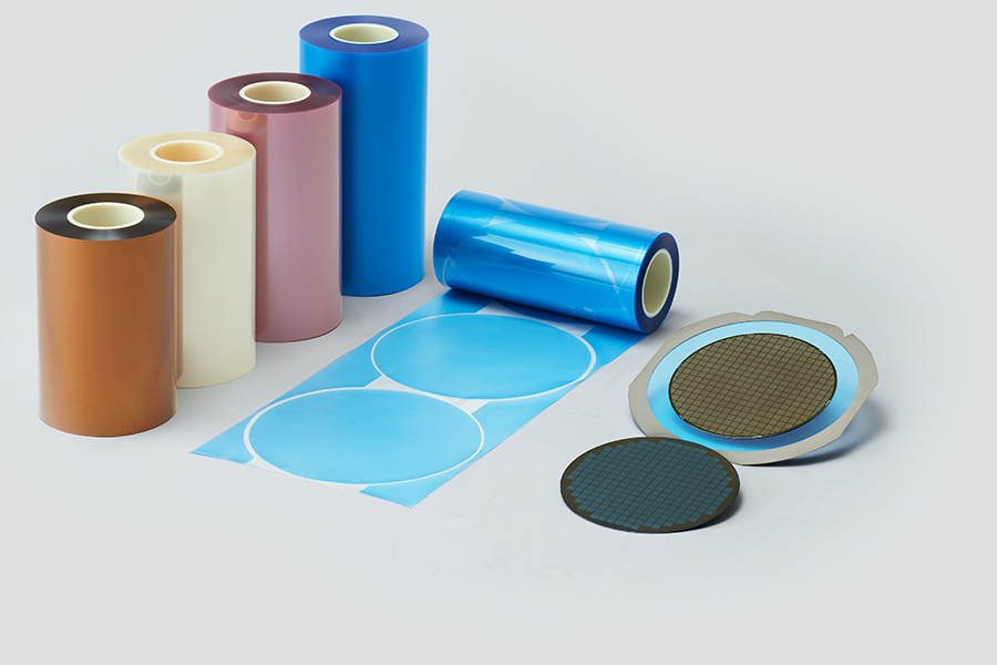
ICROS™ tape is usually 3 layers, but some tapes have more layers depending on surface construction of wafer/substrate and process requirements.

Each layer has different functions and combination of multiple layers provides various solutions for your needs.
We offer best proposal for your process from dozens of our tapes from our portfolio.


Process
Covering a broad range
of processing fields
ICROS™ tape is mainly used in semiconductor back-end process such as wafer backgrinding (BG), wafer dicing (DC) and packaging.
ICROS™ tape protects sensitive product from damage and contamination during process and supports process handling.

Application is not just for semiconductor production process but also for other products manufactured under clean environment such as sensor device, optics, MEMS and so on.


Properties / Applications
- Non-UV(PSA)

- UV tape
- Thermal
self releasing
01Tape type by peel-off
method
Non-UV(PSA)
Tape which is designed to peel-off from wafer/substrate material without UV irradiation
- Back grinding(BG)A step of semiconductor fabrication to reduce thickness of wafer. Tape required good cushioning and adhesion to prevent wafer breakage and contamination on circuit side during the process.
- Dicing(DC)A step of semiconductor fabrication to separate die (chip) from a wafer by using mechanical blade (saw). a.k.a. Sawing. Tape requires good fixation of die during the process and expandability is often required.
- Thin grindingA term generally refers to wafer or process grinding less than 100um thickness. Tape requires good cushioning and supportability to prevent wafer breakage. TAIKO™ process may be applied.
- Rinse lessPSA tape which is designed to not need cleaning process after tape peel-off.
- Halogen freeTape which comply with IEC 61249-2-21 for content rate of Chlorine (Cl) and Bromine (Br).
- PDMS freeTape using liner which does not have coated PDMS as release agent. Dimethylpolysiloxane. a.k.a. Silicone, Polyorganosiloxane.
- ECO friendlyTape which has non-solvent adhesive, and does not emit air pollutants and ecotoxic substances during tape manufacturing process.
UV tape
Tape which can be peeled off from wafer/substrate material easily after UV irradiation
- Back grinding(BG)A step of semiconductor fabrication to reduce thickness of wafer. Tape required good cushioning and adhesion to prevent wafer breakage and contamination on circuit side during the process.
- Dicing(DC)A step of semiconductor fabrication to separate die (chip) from a wafer by using mechanical blade (saw). a.k.a. Sawing. Tape requires good fixation of die during the process and expandability is often required.
- Stealth Dicing™Dicing performed by laser irradiation. The sawing width (distance between dies) is much narrower, so accurate fixation on tape is stricter compared to mechanical blade dicing. In a case of laser irradiation from backside, transparency is needed in the tape.
- DBG™/SDBG/GALDicing Before Grinding/Stealth Dicing Before Grinding/Grinding After Laser. A kind of BG and DC method for thin wafer grinding. Half-cut by mechanical blade or making modified layer by laser irrandiation is performed as first step, then die separation during wafer backgrinding. Tape requires both good encapsulation and good fixation of dies.
- Thin grindingA term generally refers to wafer or process grinding less than 100um thickness. Tape requires good cushioning and supportability to prevent wafer breakage. TAIKO™ process may be applied.
- Switching functionTape which has function to reduce its adhesion drastically when irradiating UV or heating.
- High adhesionTape which is designed to have high adhesion and tackiness on wafer.
Thermal self releasing
Tape which can be released from wafer/substrate material with zero-stress when certain temperature is applied
- Carrier handlingA handling method of thin wafer and wafer which has non-flat surface on both side like TSV wafer. Typically, glass or metal carrier supports the wafer handling with temporary bonding material like adhesive (wax) and double sided tape.
- Temporary bondingA bonding process or material for carrier handling. Adhesive (wax) or double sided tape bond carrier to wafer. In post process, adhesive (wax) is removed (debond) by solvent usually, and double sided tape is removed by its switching function.
- MoldingA step of semiconductor fabrication to encapsulate die by plastic resin. Epoxy resin is most popular resin used. Tape requires heat resistance, good adhesion and low contamination.
- Switching functionTape which has function to reduce its adhesion drastically when irradiating UV or heating.
- Fan Out packageA type of wafer level package which has extended area of I/O (Input/Output) than die area without using substrate. a.k.a. FOWLP (Fan Out Wafer Level Package). This advanced package is used for PMIC (Power Management IC), RFIC, Audio Codec, mmWave radar and so on in nowadays.
- Uniformity
- Expandability
- Transparency
- High adhesion and
Low
contamination
02Basic properties
Uniformity
Tape where thickness uniformity is controlled under strict production management
- Back grinding(BG)A step of semiconductor fabrication to reduce thickness of wafer. Tape required good cushioning and adhesion to prevent wafer breakage and contamination on circuit side during the process.
- Dicing(DC)A step of semiconductor fabrication to separate die (chip) from a wafer by using mechanical blade (saw). a.k.a. Sawing. Tape requires good fixation of die during the process and expandability is often required.
- Stealth Dicing™Dicing performed by laser irradiation. The sawing width (distance between dies) is much narrower, so accurate fixation on tape is stricter compared to mechanical blade dicing. In a case of laser irradiation from backside, transparency is needed in the tape.
- DBG™/SDBG/GALDicing Before Grinding/Stealth Dicing Before Grinding/Grinding After Laser. A kind of BG and DC method for thin wafer grinding. Half-cut by mechanical blade or making modified layer by laser irrandiation is performed as first step, then die separation during wafer backgrinding. Tape requires both good encapsulation and good fixation of dies.
- Thin grindingA term generally refers to wafer or process grinding less than 100um thickness. Tape requires good cushioning and supportability to prevent wafer breakage. TAIKO™ process may be applied.
- TTVTotal Thickness Variation. A term or an indicator of semiconductor wafer thickness. Tape is required to have both thickness uniformity and encapsulation on uneven surface of wafer to achieve good TTV.
- Memory deviceA generic name of data storage device such as NAND flash, DRAM and SRAM.
- Power deviceA generic name of device which work for switching or rectifying power electronics such as diode, MOSFET (Metal Oxide Semiconductor Field Effect Transistor) and IGBT (Insulated Gate Bipolar Transistor).
Expandability
Tape which uses flexible material in order to withstand mechanical transformation
- Dicing(DC)A step of semiconductor fabrication to separate die (chip) from a wafer by using mechanical blade (saw). a.k.a. Sawing. Tape requires good fixation of die during the process and expandability is often required.
- Stealth Dicing™Dicing performed by laser irradiation. The sawing width (distance between dies) is much narrower, so accurate fixation on tape is stricter compared to mechanical blade dicing. In a case of laser irradiation from backside, transparency is needed in the tape.
- Pick upA step of semiconductor fabrication to remove dies from tape after dicing. Tape requires good elongation to withstand push up by needle.
Transparency
Tape which is suitable for optical inspection or laser processing through the tape
- Back grinding(BG)A step of semiconductor fabrication to reduce thickness of wafer. Tape required good cushioning and adhesion to prevent wafer breakage and contamination on circuit side during the process.
- Dicing(DC)A step of semiconductor fabrication to separate die (chip) from a wafer by using mechanical blade (saw). a.k.a. Sawing. Tape requires good fixation of die during the process and expandability is often required.
- Stealth Dicing™Dicing performed by laser irradiation. The sawing width (distance between dies) is much narrower, so accurate fixation on tape is stricter compared to mechanical blade dicing. In a case of laser irradiation from backside, transparency is needed in the tape.
- Optical inspectionA generic name of inspection performed optically. a.k.a. AOI (Automated Optical Inspection). Transparent tape is available for inspection of wafer front side through the tape.
High adhesion and Low contamination
Tape which has both properties by our polymerization technologies
- Back grinding(BG)A step of semiconductor fabrication to reduce thickness of wafer. Tape required good cushioning and adhesion to prevent wafer breakage and contamination on circuit side during the process.
- Dicing(DC)A step of semiconductor fabrication to separate die (chip) from a wafer by using mechanical blade (saw). a.k.a. Sawing. Tape requires good fixation of die during the process and expandability is often required.
- Stealth Dicing™Dicing performed by laser irradiation. The sawing width (distance between dies) is much narrower, so accurate fixation on tape is stricter compared to mechanical blade dicing. In a case of laser irradiation from backside, transparency is needed in the tape.
- DBG™/SDBG/GALDicing Before Grinding/Stealth Dicing Before Grinding/Grinding After Laser. A kind of BG and DC method for thin wafer grinding. Half-cut by mechanical blade or making modified layer by laser irrandiation is performed as first step, then die separation during wafer backgrinding. Tape requires both good encapsulation and good fixation of dies.
- Metal Lift-offA step of semiconductor fabrication that removes unnecessary portion of metal and resist pattern from metalized wafer surface. Tape is used to remove and collect precious metal like gold for Dry Lift-off method. Dry lift-off enables less chemical, less metal waste and shorter process time than Wet method.
- High adhesionTape which is designed to have high adhesion and tackiness on wafer.
- Bumped waferA generic name of wafer which has bump shaped electrode on surface. Bump shape, height and density are depends on package type. e.g. solder bump, Cu-pillar for Flip chip and WL-CSP, and gold bump for LCDD (LCD Driver IC)
- Bump
encapsulation - Heat
resistance - Chemical
Resistant - Anti ESD
03Functional properties
Bump encapsulation
Tape which has encapsulation function to protect designs laid out on surface of wafer / substrate material during manufacturing process
- Back grinding(BG)A step of semiconductor fabrication to reduce thickness of wafer. Tape required good cushioning and adhesion to prevent wafer breakage and contamination on circuit side during the process.
- Dicing(DC)A step of semiconductor fabrication to separate die (chip) from a wafer by using mechanical blade (saw). a.k.a. Sawing. Tape requires good fixation of die during the process and expandability is often required.
- Stealth Dicing™Dicing performed by laser irradiation. The sawing width (distance between dies) is much narrower, so accurate fixation on tape is stricter compared to mechanical blade dicing. In a case of laser irradiation from backside, transparency is needed in the tape.
- DBG™/SDBG/GALDicing Before Grinding/Stealth Dicing Before Grinding/Grinding After Laser. A kind of BG and DC method for thin wafer grinding. Half-cut by mechanical blade or making modified layer by laser irrandiation is performed as first step, then die separation during wafer backgrinding. Tape requires both good encapsulation and good fixation of dies.
- High adhesionTape which is designed to have high adhesion and tackiness on wafer.
- TTVTotal Thickness Variation. A term or an indicator of semiconductor wafer thickness. Tape is required to have both thickness uniformity and encapsulation on uneven surface of wafer to achieve good TTV.
- Flip chip (FC)A type of die connection method to substrate or a generic name of package known also by FC-BGA (Flip Chip Ball Grid Aray). FC enables faster processing speed and saving foot print of package than wire bonding package. FC is mainly adopted to processors such as MPU, GPU, BB (Base Band processor) and AP.
- WL-CSPWafer Level Chip Scale Package. A type of package which die can be mounted on PCB directly. The solder bump is bigger than FC bumps in general. WL-CSP is used for PMIC (Power Management IC), RFIC, Audio Codec and especially mobile appilications.
- TSVThrough Silicon Via. A type of connection method for multiple dies stacking in a package. TSV is mainly adopted to advanced device such as CIS (CMOS Image Sensor) and HBM (High Bandwidth Memory). Since TSV wafer has bumps on both side, carrier handling or bump encapsulation tape are required during processing and handling.
- MEMSMicro-Electro-Mechanical System. A type of device or technolgy of micromechatronics and microsystem. MEMS is not a semiconductor device but use semiconductor manufacturing technology and process.
Heat resistance
Tape which can withstand process with high temperature
- Back grinding(BG)A step of semiconductor fabrication to reduce thickness of wafer. Tape required good cushioning and adhesion to prevent wafer breakage and contamination on circuit side during the process.
- Dicing(DC)A step of semiconductor fabrication to separate die (chip) from a wafer by using mechanical blade (saw). a.k.a. Sawing. Tape requires good fixation of die during the process and expandability is often required.
- Final testA generic name of semiconducotor test after dicing. In automotive application, Tri-temperature test which apply from negative(-) 40 deg C to 150 deg C is required. Frame handling wafer level test is available by our Heat resistant DC tape.
- ReflowA step of semiconductor fabrication to make solder bumps on dies. Also called "Reflow soldering", "Bumping reflow". Tape is required to withstand up to 260 deg C.
- DAFDie Attach Film. DAF is laminated on wafer back grinded side to fix die onto lead frame in post process. Tape is required to withstand DAF curing process.
- MoldingA step of semiconductor fabrication to encapsulate die by plastic resin. Epoxy resin is most popular resin used. Tape requires heat resistance, good adhesion and low contamination.
- EtchingA step of semiconductor fabrication to remove layer from wafer surface chemically. Tape is required to withstand etchants (mostly acid) and the coating process (spin coating/dipping).
- Fan Out packageA type of wafer level package which has extended area of I/O (Input/Output) than die area without using substrate. a.k.a. FOWLP (Fan Out Wafer Level Package). This advanced package is used for PMIC (Power Management IC), RFIC, Audio Codec, mmWave radar and so on in nowadays.
- Power deviceA generic name of device which work for switching or rectifying power electronics such as diode, MOSFET (Metal Oxide Semiconductor Field Effect Transistor) and IGBT (Insulated Gate Bipolar Transistor).
Chemical resistance
Tape which can withstand process that uses chemicals such as solvent and acid
- Back grinding(BG)A step of semiconductor fabrication to reduce thickness of wafer. Tape required good cushioning and adhesion to prevent wafer breakage and contamination on circuit side during the process.
- Dicing(DC)A step of semiconductor fabrication to separate die (chip) from a wafer by using mechanical blade (saw). a.k.a. Sawing. Tape requires good fixation of die during the process and expandability is often required.
- Carrier handlingA handling method of thin wafer and wafer which has non-flat surface on both side like TSV wafer. Typically, glass or metal carrier supports the wafer handling with temporary bonding material like adhesive (wax) and double sided tape.
- Temporary bondingA bonding process or material for carrier handling. Adhesive (wax) or double sided tape bond carrier to wafer. In post process, adhesive (wax) is removed (debond) by solvent usually, and double sided tape is removed by its switching function.
- EtchingA step of semiconductor fabrication to remove layer from wafer surface chemically. Tape is required to withstand etchants (mostly acid) and the coating process (spin coating/dipping).
- SRDA generic name of cleaning process of semiconductor fabrication. Spin Rinse Dry.
- Power deviceA generic name of device which work for switching or rectifying power electronics such as diode, MOSFET (Metal Oxide Semiconductor Field Effect Transistor) and IGBT (Insulated Gate Bipolar Transistor).
- TSVThrough Silicon Via. A type of connection method for multiple dies stacking in a package. TSV is mainly adopted to advanced device such as CIS (CMOS Image Sensor) and HBM (High Bandwidth Memory). Since TSV wafer has bumps on both side, carrier handling or bump encapsulation tape are required during processing and handling.
Anti-ESD
Tape which has conductive property to allow electric discharge
- Back grinding(BG)A step of semiconductor fabrication to reduce thickness of wafer. Tape required good cushioning and adhesion to prevent wafer breakage and contamination on circuit side during the process.
- Dicing(DC)A step of semiconductor fabrication to separate die (chip) from a wafer by using mechanical blade (saw). a.k.a. Sawing. Tape requires good fixation of die during the process and expandability is often required.
- ESDElectro-Static Discharge. ESD failure causes damage on integrated circuit which is especially a concern for advanced node device.
- Flip chip (FC)A type of die connection method to substrate or a generic name of package known also by FC-BGA (Flip Chip Ball Grid Aray). FC enables faster processing speed and saving foot print of package than wire bonding package. FC is mainly adopted to processors such as MPU, GPU, BB (Base Band processor) and AP.
[Trademarks and registered trademarks of respective companies]
*1: “Stealth Dicing” is a trademark or registered trademark of Hamamatsu Photonics K.K.
*2: “DBG” is a trademark or registered trademark of LINTEC Corporation, DISCO Corporation and Kioxia Corporation.
*3: “TAIKO” is a trademark or registered trademark of DISCO Corporation
Why ICROS™Tape?


Customer support system
Our global network offers on-time technical solutions and supports customer’s business worldwide. Our R&D supports customer’s process optimization, material analysis, and tape development using equipements in our laboratory, and collaborate with external machine makers to provide best solution.
Proven and Trusted Brand
We started development of tape for semiconductor process in 1980s, and ICROS™ tape commercialized in 1987.
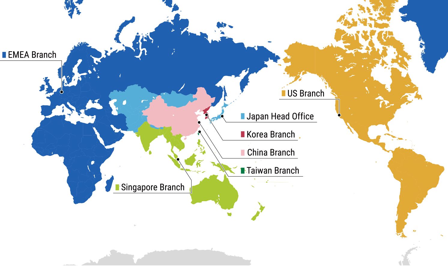
ICROS™ tape is now used worldwide, and our customers are located in 25+ countries and region.
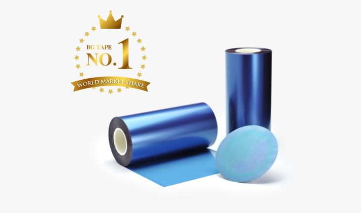
We own the No.1 global market share* of wafer backgrinding tape.
*according to our research, as of November 2020


Contributions to the Environment
Some ICROS™ tapes use non-solvent adhesive so it does not emit no air pollutants and ecotoxic substances during tape manufacturing process.
We continue to make an active contributions to the environment.
Global Network
Tap the icon to display the base information.